A range of test technologies is available, including in circuit test (ICT), flying probe test (FPT), functional test (FT), automated optical inspection (AOI) and boundary scan. Each has its pros and cons, but one factor is decisive: cost. Contributory factors to cost include: test preparation; test execution; and failure search.
However, decisions should not always be based on cost; analysing the specifications is important, as each test technology has implementation problems.
The disadvantages of these test techniques include:
FT:
• intensive test program creation costs
• high troubleshooting costs; troubleshooting must be performed by well trained personnel
• Practically impossible to test all functions and get 100% coverage.
ICT:
• high test fixture development costs
• extra costs with layout changes
• expensive to storage and maintain adaptors
• probe placement becomes more difficult as pcb trace density increases
• access to high lead count bgas via nails is nearly impossible.
AOI:
• Not possible to detect faults beneath components
• electric faults cannot be detected.
FPT:
• Long test times due to the sequential contacting of test points
• maintenance costs for worn contact pins and moved mechanical components.
Test friendly design
Test friendly design requires the development of a test concept with all required hardware and software elements in the unit to be tested. This is characterised as 'test oriented layout' or, more commonly, design for testability (DFT).
The trend to digital technology is obvious and must be considered when choosing the right test strategy because of the particular problems of testing digital circuits: test pattern generation and test verification. Test pattern generation produces stimulus signals for a circuit, in order to prove correct function. Test verification determines the circuit's response.
Simultaneously, automatic test pattern generation and test verification have become more difficult due to increasing pcb complexity. This can be clarified using functional test as an example.
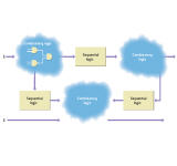
Assuming that each digital circuit comprises sequential and combinatorial elements (see fig 1), the minimum number of test vectors (Q) for 100% functional test, according to Moore and McCluskey, is: Q = 2exp(x+y) where x is the number of inputs and y is the number of storage elements (sequential circuit parts).

Testing a circuit with 25 inputs (x) and 50 internal latches (y) at a rate of 100ns per step would take 10exp7 years.
This problem can be avoided by designing circuits which are more efficiently testable – using sequential circuit parts. This means the circuit must be designed to be tested with acceptable fault coverage and an acceptable test time. Furthermore, it should overcome the problem of test access.
Subdividing DFT
DFT must be subdivided into ad hoc and structured design elements. The ad hoc design contains the partitioning, the importation of additional test points and the use of bus architectures. Partitioning means breaking the circuit into parts which are easier to test. The sum of the effort to test these part pcbs is considerably less than the effort of testing the entire circuit. Bus architectures simplify testability by selective activation of individual bus participants.
Structured design aims to reduce sequential complexity in order to simplify test pattern generation and test verification. It does this by creating ways to control and observe sequential machine states. Methods, that implement these circuit types are called passive test aids.
One passive test aid is the scan path method. Using this, circuits with sequential storage elements can be subdivided into observable and controllable combinatorial circuit parts. The storage elements' internal states must be controllable and observable. This can be achieved by interconnecting internal storage elements and shift registers to enable the serial insertion of test items and the serial read out of test answers.
The classic among these methods is level sensitive scan design (LSSD, see fig 2). Developed by IBM for mainframe computers in the 1960s, LSSD is based on the extension of functional storage elements to shift register elements – or shift register latches (SRL).
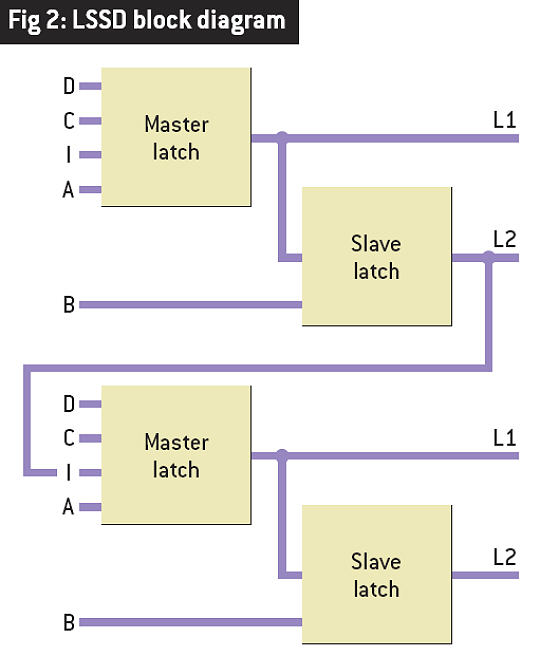
In normal operation, the SRL works as a latch (A=B=0), with data input D, clock input C and data output L1. In test mode, it functions as a shift register cell (C=0). The shift data input I is connected with the shift data output L2 of the previous cell, with data switched from L2 to the next cell's I. The clock inputs A/Master Clock and B/Slave Clock alternate and cause the shift.
The scan path method shows that complex sequential circuits can decompose into manageable, purely combinatorial circuits. Since combinatorial circuits require substantially fewer test vectors, test expenditure and testing time are significantly less.
Figure 3 shows the example circuit decomposes into combinatorial blocks, which are tested partly by the external lines, but also – and this is important – by the circuit's internal sequential logic. The disadvantage of the sequential logic is turned into an advantage by its use as part of the test machinery.

Application to pcbs
DFT has its roots in circuit technology, so it is logical that it should also apply to pcbs; if the technology is applicable for circuits, it must be transformed to assemblies.
Test cells are required between the circuits and should be switchable as shift chains, as well as controllable and readable via a few lines. If these test points are placed in the lines, they are used for in circuit test. But increasing pcb complexity demands the integration of these test points in components to clear additional space for nets.
This 'test friendly' requirement is met by boundary scan, which has evolved to a standardised test of components and their interconnection networks. Boundary scan is possibly the most resourceful test technique which detects the failure location, sets thousands of test points – if necessary under bgas – and needs only four lines. While ICT is only possible with specially constructed adaptors, a boundary scan test is already useful if there is at least one boundary scan component on board.
Boundary scan essentially means testing at an ic's periphery. Besides core logic and contact points, some additional logic is implemented in an ic and test points are integrated between core logic and physical pins.
Boundary scan is simply and universally adaptable and one can argue the technology supports products through their entire life cycle. In the design stage, tests are possible using CAD data, which means the test pattern created for design verification can be reused for prototype debug and fabrication test. This is important – especially when designing complex assemblies – because future testability has to be considered.
Time and effort required for testing is reduced; only a few days or even hours are required to generate test programs, compared with the efforts which accompany in circuit test or functional test.